Electrostatic discharge (ESD) is as old as time. It has, however, become a major phenomenon as the world moves forward with technology advancement. Internal circuits are getting smaller by the day, and more and more devices are advancing. Electronic designing has become one of the major technological things for engineers to do. Every designer using PCB and other components today is no longer all about using anti-static mats and anti-static wristwatches for protection. Electrostatic discharge (ESD) is a big threat that requires enough protection, especially during the time of designing.
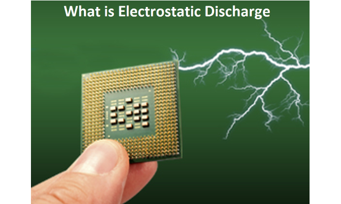
What is Electrostatic Discharge?
Sometimes, when two objects encounter each other, there is an unintended flow of spontaneous electricity or a breakdown of dielectric between the objects. The contact may not necessarily be physical, but objects coming together in close proximity can cause this flow. Dielectric occurs over the air with consumer products. This spontaneous flow of electricity, known as electrostatic discharge (ESD), can unintentionally wreak a lot of havoc. One of the most common forms of ESD is lightning. Lightning occurs when the earth and the clouds form a capacitor.
ESD does not affect only electronics. This phenomenon affects a number of other industries, too, like pharmaceutical, textiles, petrochemical, plastics and many more. For PCB designers, ESD can be catastrophic if left unchecked.
How ESD Affects the PCB
Whether it is during production or you have your PCB in your hands, any PCB is prone to the dangers of ESD. Some parts of the PCB components might be tough enough to withstand ESD, but there are others like internal circuits and semiconductors that easily damage by the slightest change in current. Even if the damage does not cause major setbacks immediately, they eventually stagnate electric equipment and components that are too sensitive; and this can happen days or months down the road if the problem is not rectified or noticed in time. This can be a huge disadvantage for any company or institution that relies on these applications.
Every component of PCB design can affect the protection of ESD on the board. These elements – routing, traces, spacing and component placement – need early checking during the design process to avoid these setbacks. If left unchecked, you might have to redesign your PCB from scratch, and fix issues of component placements and routing.
What Causes ESD?
ESD builds up when two materials come into contact with each other and later separate. The continuous process of contact and separation transfers starts an atomic reaction. Atoms, when in a balanced state, have the same number of electrons (-) and the same number of protons (+). Consistent and continuous contact makes everything go out of balance.
On a PCB, ESD originates from the interface of the user or at a completely different input. Activities on the PCB, like touching the components, pushing keys, buttons or screen, and plugging cables in, always results in discharge.
How to Protect your PCB from ESD
It is very important that you protect the PCB from any connections that are external, to minimize interaction with your design by users. Electrostatic discharge penetrates the board every time there is a cable plugged in or out, every time a button gets pushed or at any other time an activity takes place with your PCB.
Use only one copper land to attach all your PCB connectors, and separate the pad and the PCB ground to avoid any shock routing to other board components. Use only the best practices for grounding; and when connecting to the ground, only use TVS for every external connection and make a reduction of the circuit loops.
ESD is a problem that you can stop from destroying your PCB.